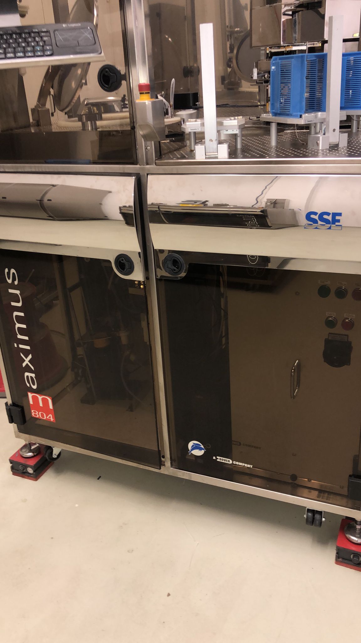
SSE Maximus Single Coater Closed Cover Chuck with max. 4 Hotplates and 1 Coolplate.


Manufacturer: Neuberger
Type: Degistor AZ 180
Year of manufacture: 2018
Dimensions (l/w/h): ca, 1800 x 1000 x 2500 mm
Weight(kg): estimated 750 kg
General function: Fume cupboard with integrated ventilation device for toxic fume, vapors and dusts and included pump station
For immediate sale one Neuberger Degistor AZ 180. The cupboard is fully functional and can be inspected in Austria after consultation.

For further further questions about the history of the machine feel free to contact us via email or phone:
+49 170 2844435
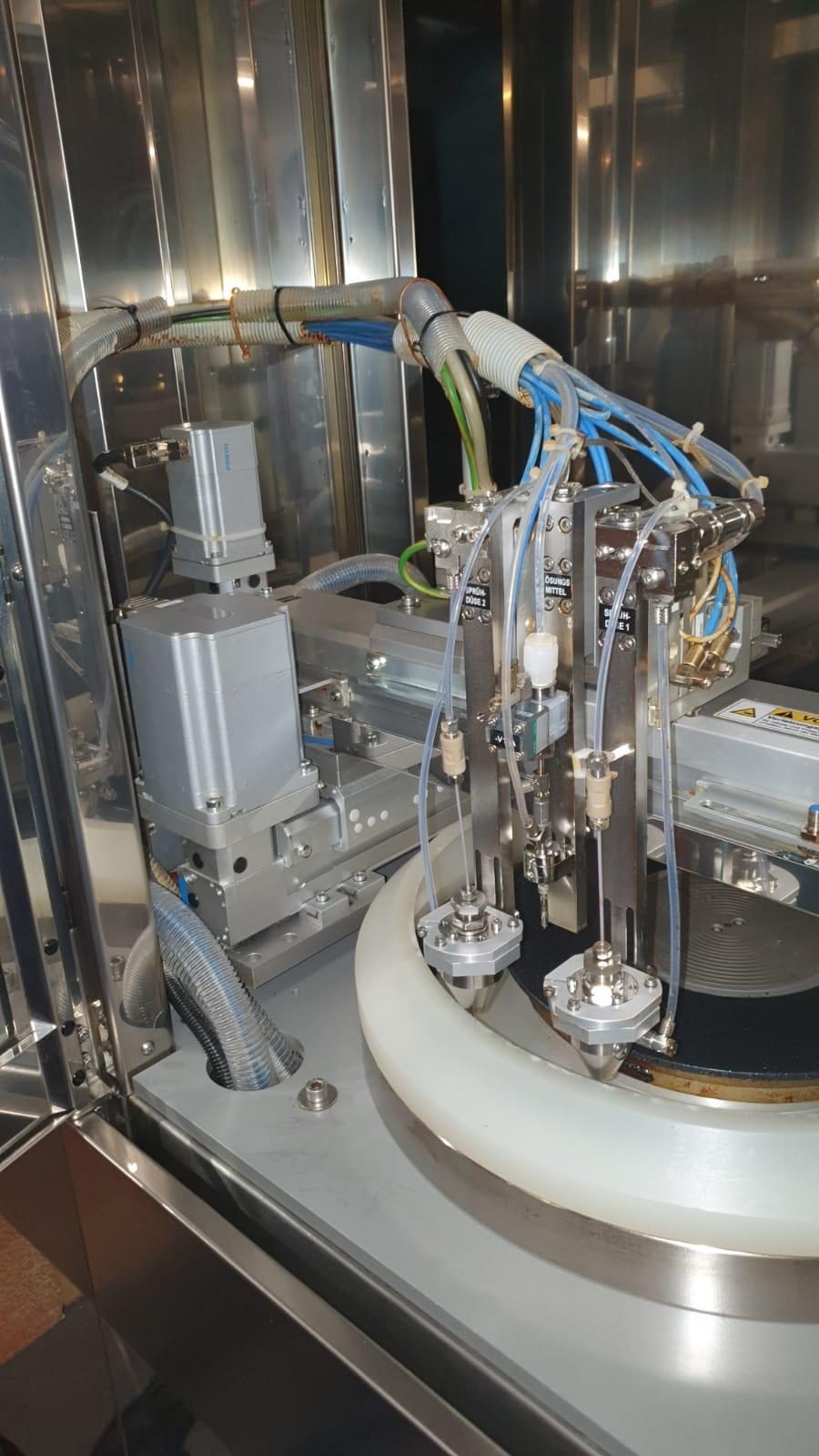
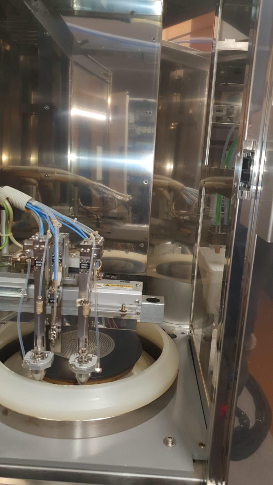
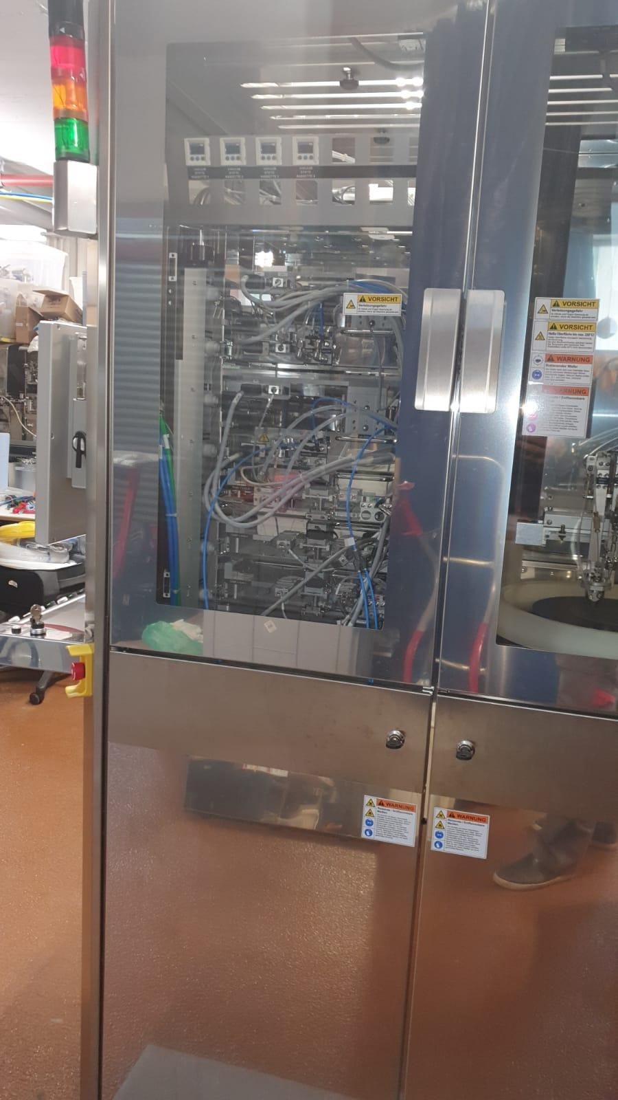
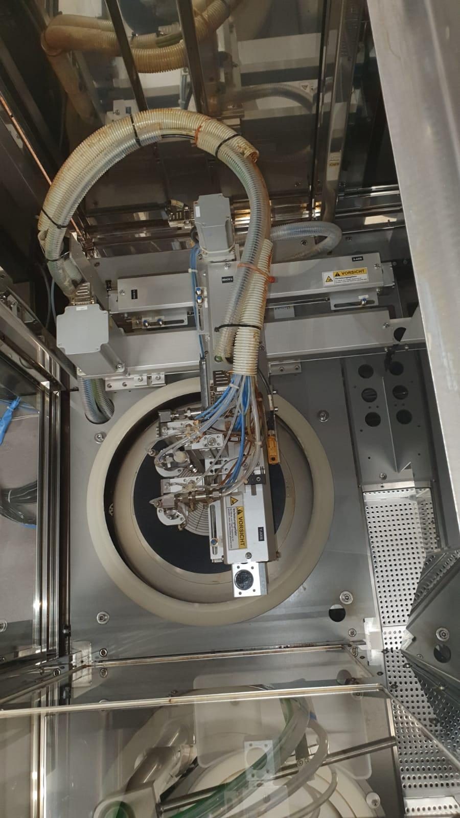
Manufacturer: Siconnex
Type: Batchspray Acid for 300mm for 25 Wafers/Square Substrates
Year of manufacture: 2018
Dimensions (l/w/h): ca, 2000 x 1200 x 2000 mm
Weight(kg): estimated 1500 kg
Type of PLC: Beckhoff
General function: 12″ rotating batchspray machine for etching and cleaning with acids os bases (closed system). Currently the tools are set up for 12″ square substrates. The tool can be upgraded to process Wafers. The machines are very young and come from a pilot line. Excellent condition.
We have 2 systems for immediate sale. Both Siconnex Batchspray acid tools are fully functional an can be inspected in Austria after consultation.
If you have further questions about the history of the tools, please feel free to contact us via form or phone:
+49 170 2844435
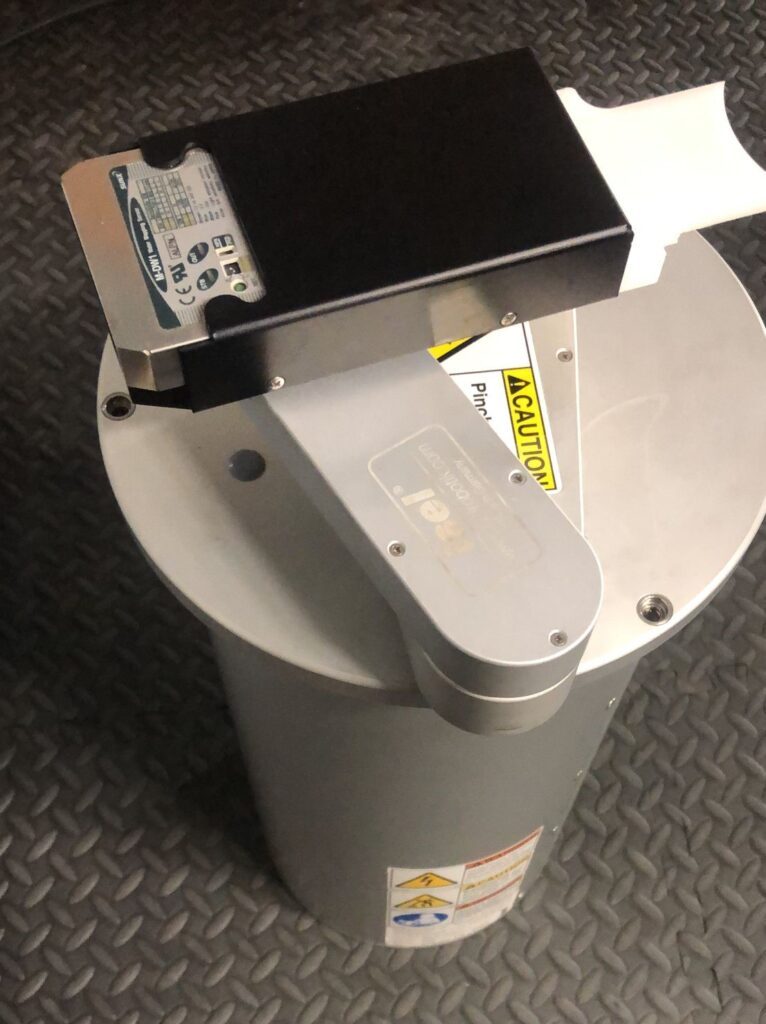
For sale: Here is an ISEL IWH-TA10S10F-1 Wafer Handler manufactured in 2009.
The robot is fully functional and comes with the pictured mapping sensor. As the robot comes from a Siconnex Vertical Developer, we also have a corresponding guide rail and controller. The robot has been in use for around 4 years in total. The robot was taken out of production in 2018. The robot is in excellent condtion.
The robot is immediately available. If you have any questions, please feel free to contact us: Cell number:
+49 170 2844435


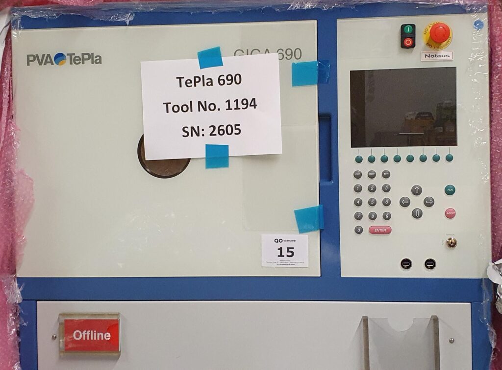
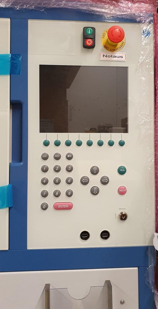
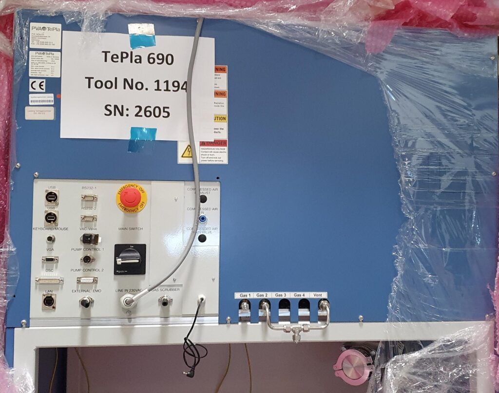
We are selling here a GIGA 690 from PVA TePLA.
The GIGA 690 is a MICROWAVE PLASMA SYSTEM. Further information:
The GIGA 690 was 4 years in production and is in a realy good condition. Year of manuafcture mid 2015 and taken out of production in early 2019.
The Machine is currently crated as can be seen, but can easily be prepared for inspection. The location is in Germany. For further information please contact us.
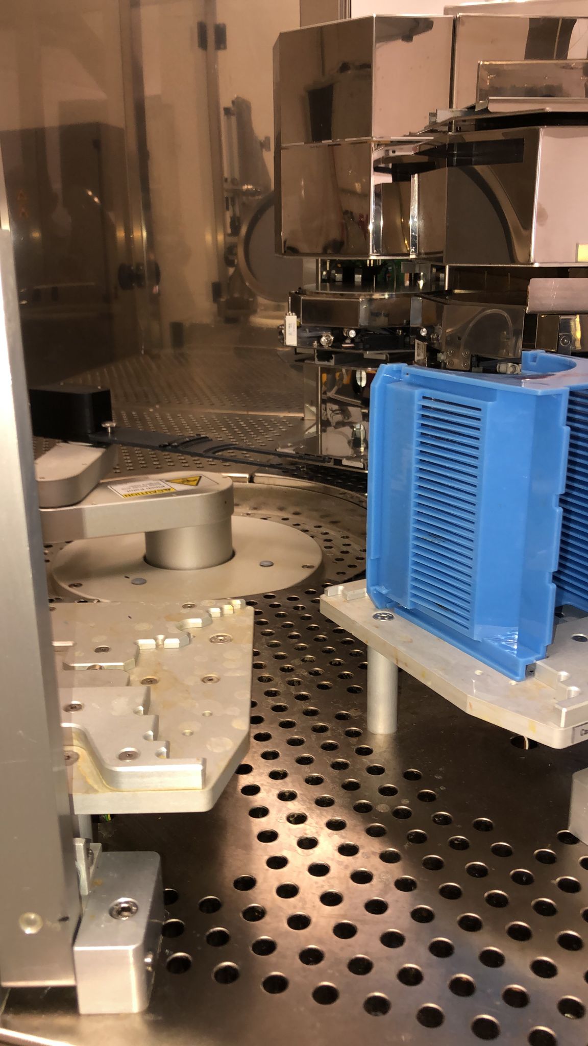
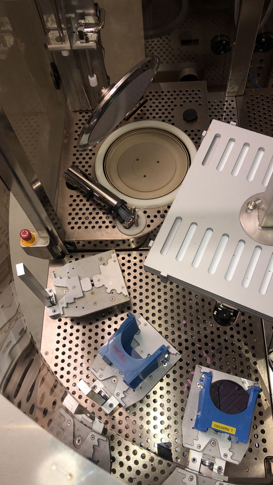
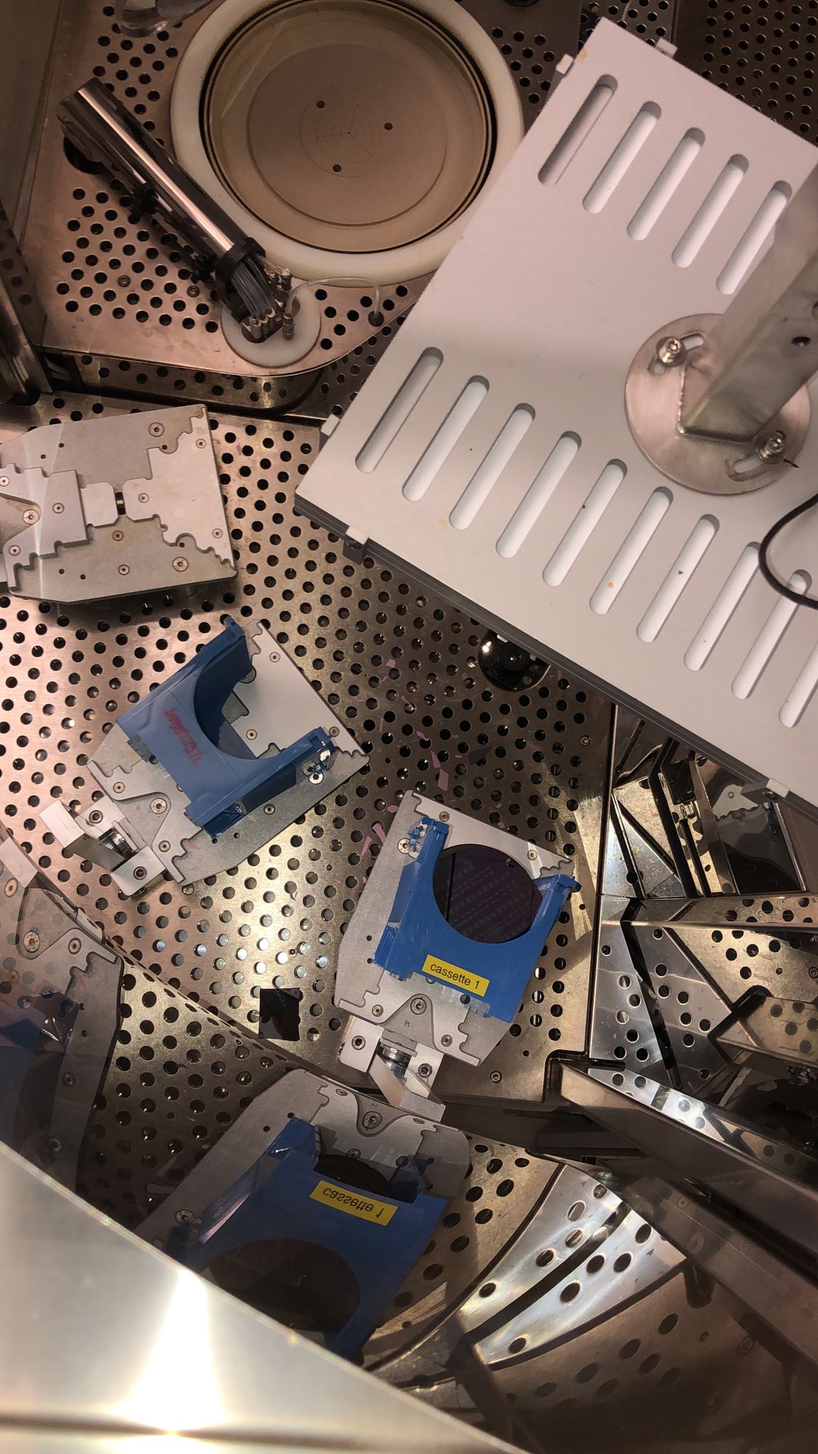
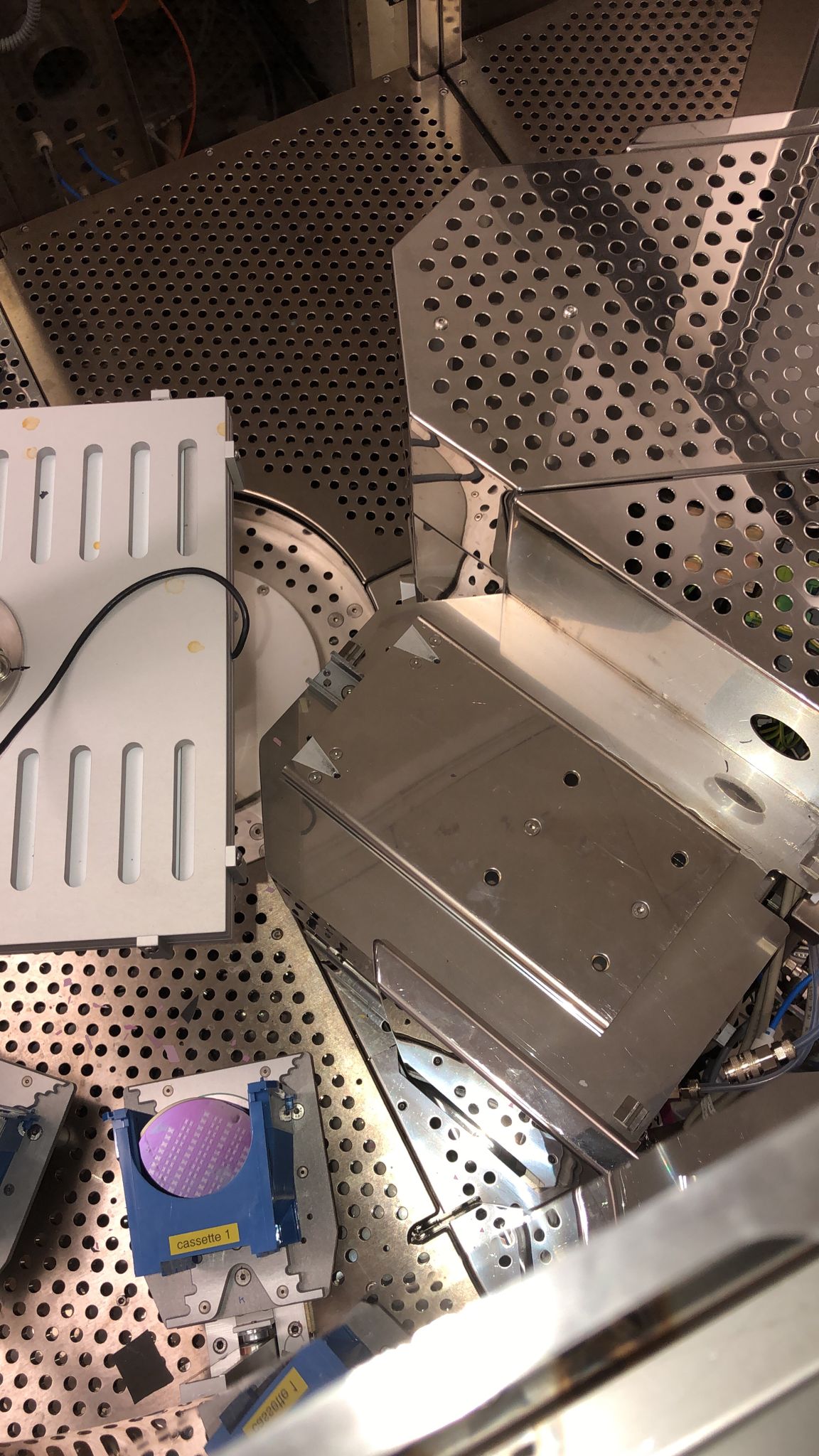
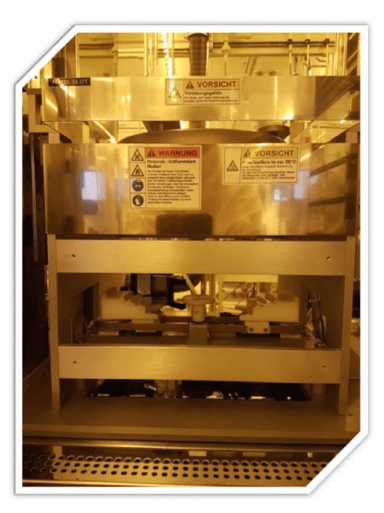
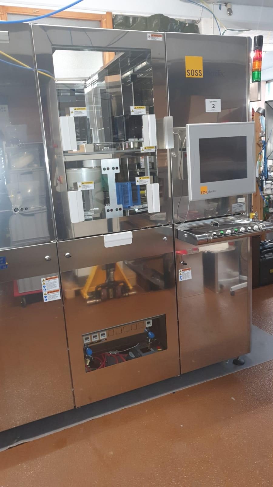
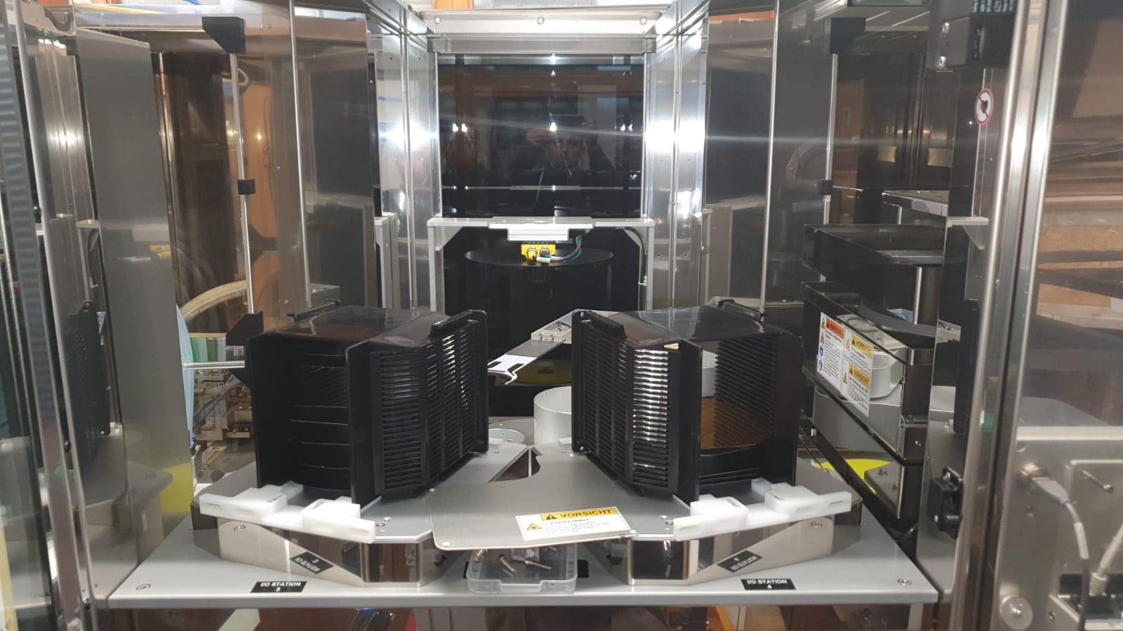
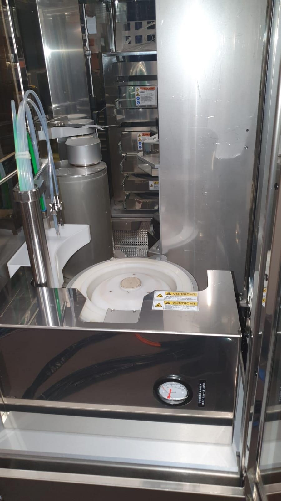
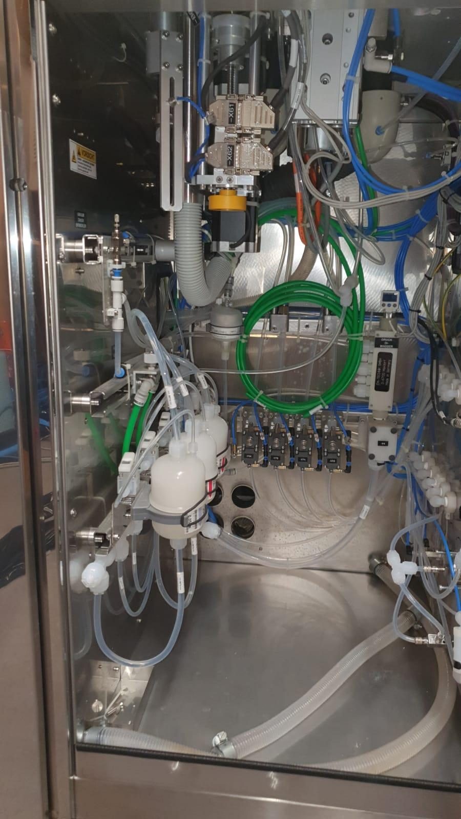
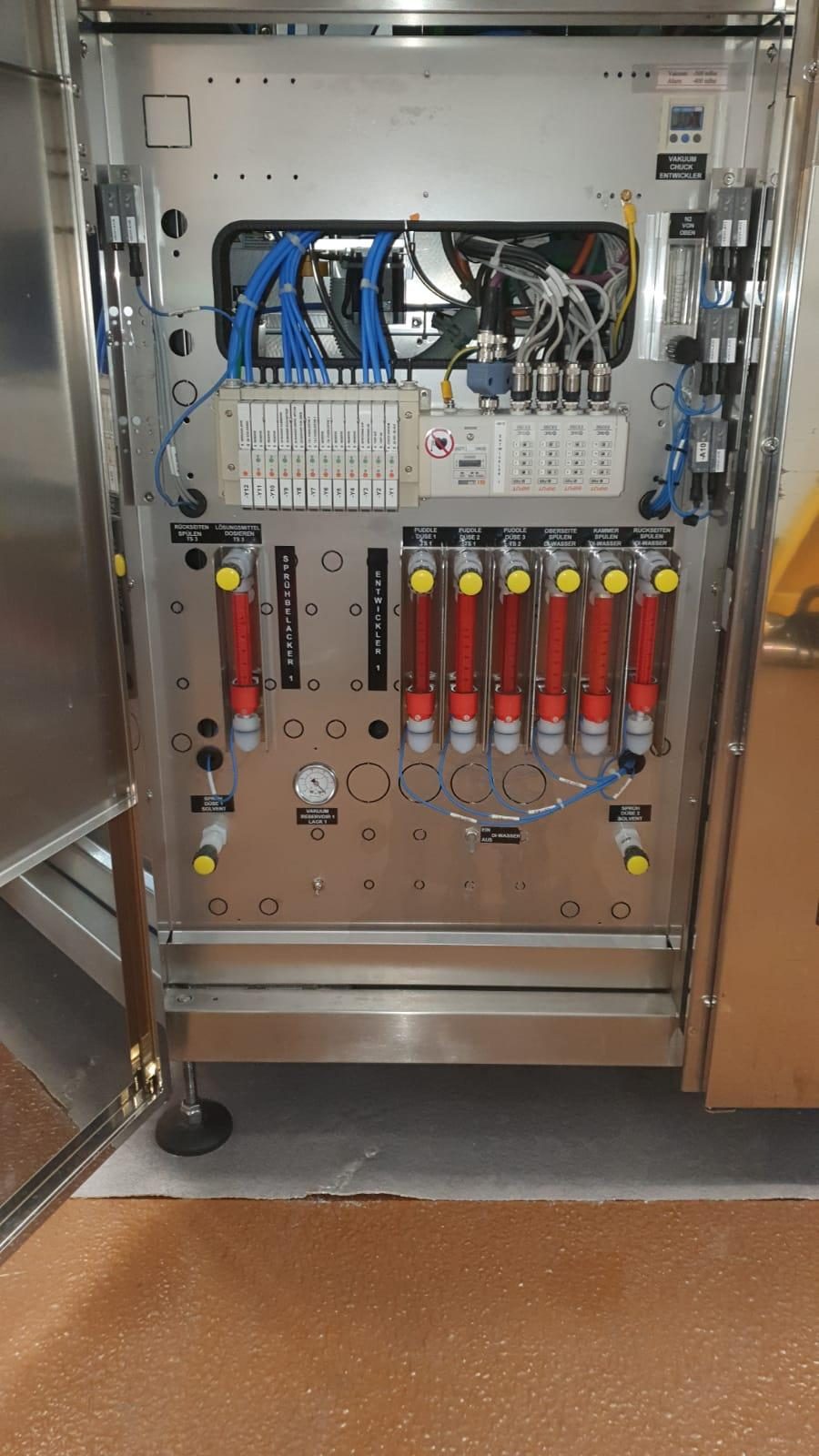
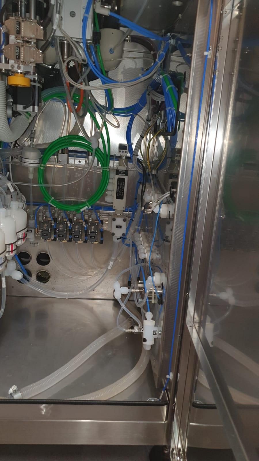
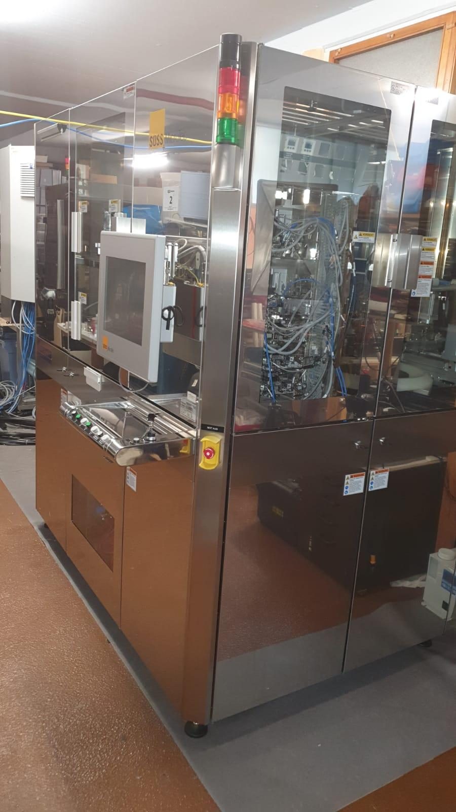
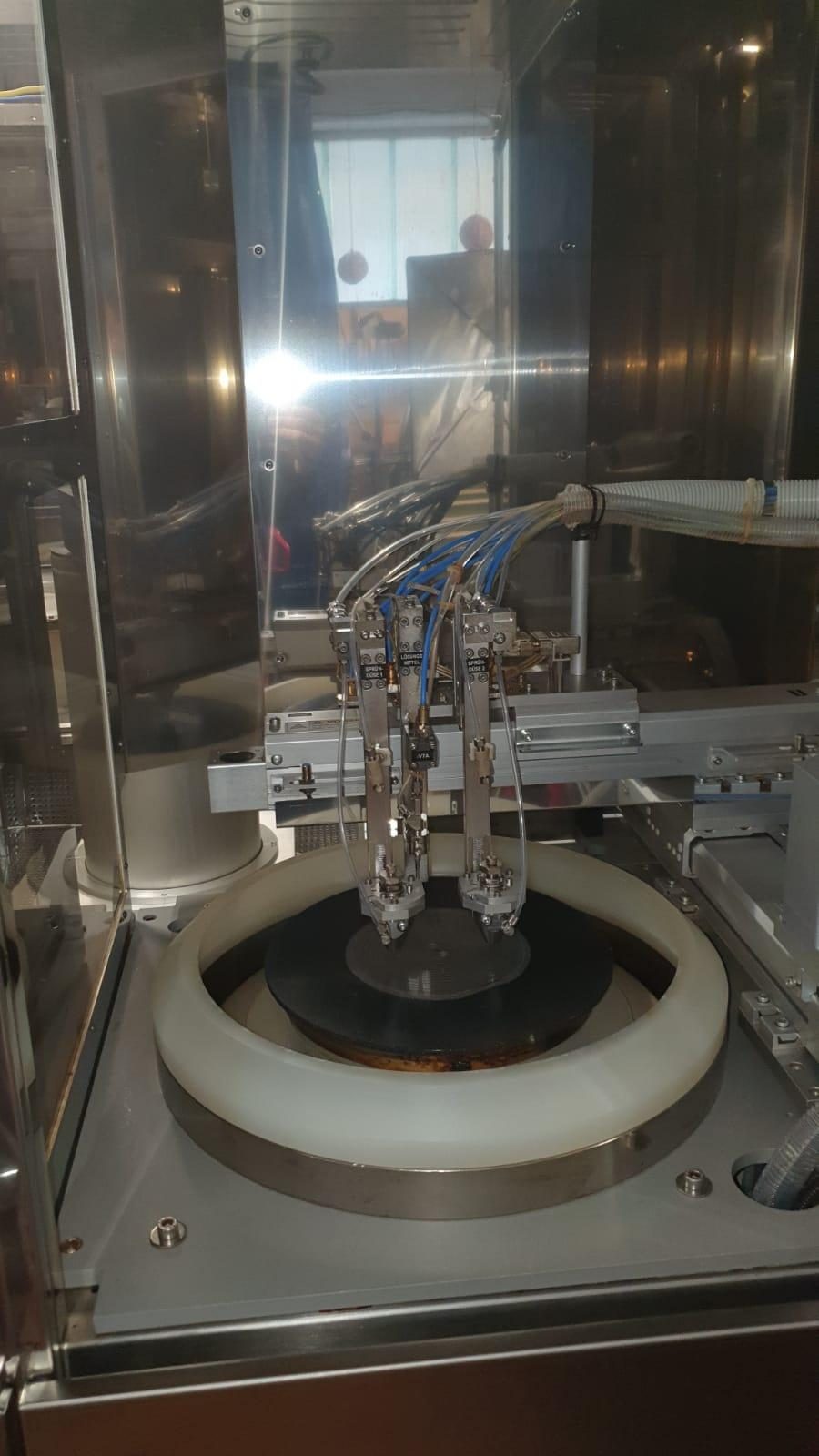
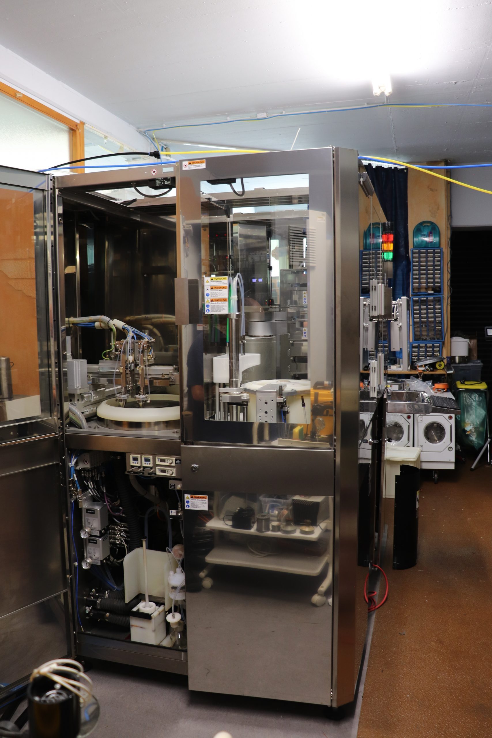
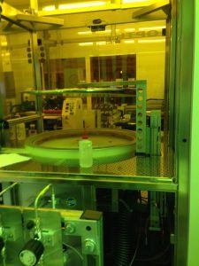
We have 1 Suss Gamma Cluster Coater-Developer Machine for immediate sale.
Installation, Service and Spare Parts are available.
The machine is fully functional and can be inspected on request. For further information please contact us.


We are selling here a Wafer Disco Mounter.
The Mounter is fully functional. Please contact us for further information.


Manufacturer: Suss Microtec Year of manufacture: 2013 / 2014
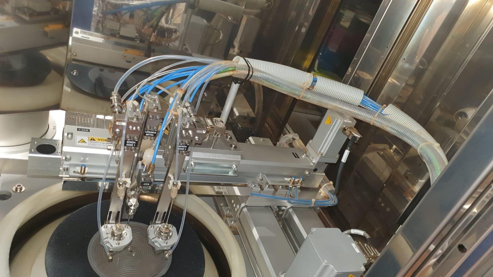
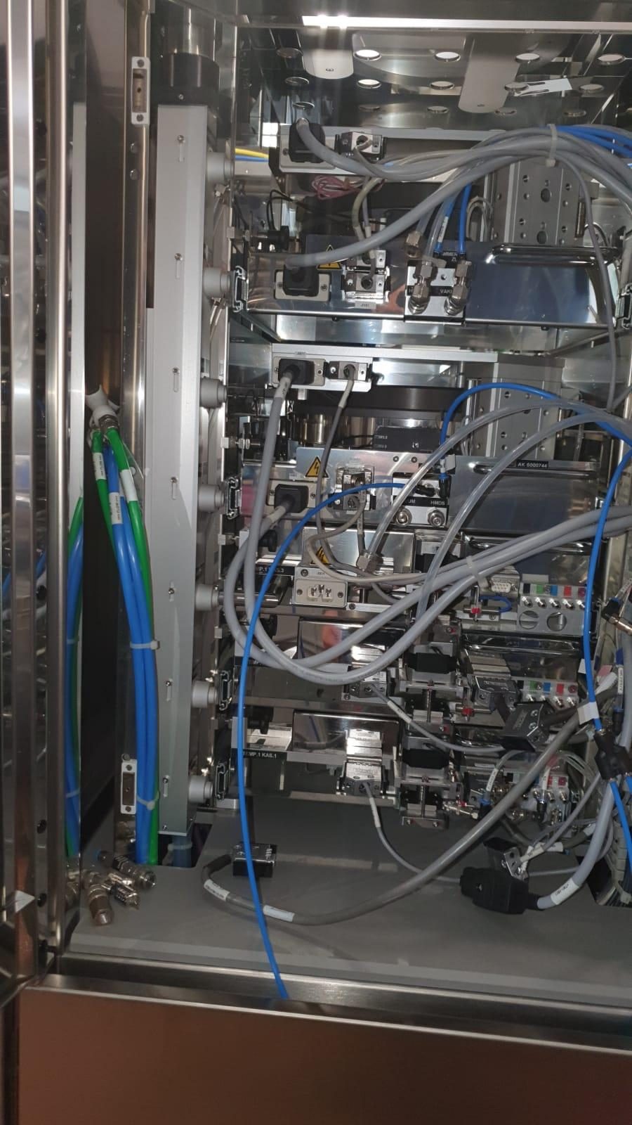
Model: Suss Gamma Cluster System: Coater- Developer with Hotplates and Coolplates
Condition: Excellent, complete system, serviced during production period by Suss Microtec
working horse,
Wafer size: 6″ & 8″mm wafers.
Configuration: 4 Cassettes
2 ea Spray Coat Stations / Note: The Spray Coat Stations can be upgraded to
Spin Coaters
1 ea Developer Station
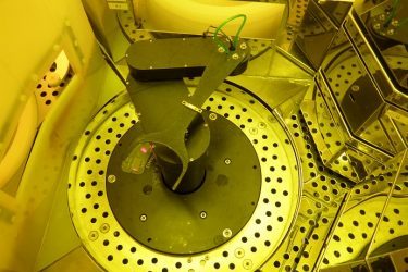
1ea Sankyo Wafer Handling Robot
1 ea Optical Centering Station
2 ea HMDS Hotplates 250 °C
1 ea Standard proximity Hotplate 250 °C & 2 ea Coolplates.
3 ea Media Cabinets with a total of 6 pressurized tanks
1 ea Electrical Cabinet
Options: If needed configuration of hotplates and coolplates can be modified to customer requirements.
Installation, Technical Support, spare parts and process support available.
The machine was in production from 2014 to early 2019. From 2019 until today the machine is used in our show room in Remseck Germany. 3 other Spray Coater – Developer Cluster Tools are available. Property of APEX Semiconductor GmbH.


Since LED became an attractive alternative for general lighting, the market demand for higher brightness, higher efficiency and lower costs was the motivation for improving the LED tech – nology. Whereas an increase in brightness and efficiency is mostly a question of the LED chip design, a reduction of the costs is in the focus of the manufacturing technology. As Haitz stated in 2000, the cost per lumen falls by a factor of 10 every decade. This, later referred to as Haitz’s law [1] , is considered the LED counterpart to Moore‘s law, which states that the number of transistors in a given integrated circuit (IC) doubles every 18 to 24 months. Both laws rely on the process optimization in the production of semi – conductor devices. However, at the IC industry it is recognized that an increase in the number of transistors come along with higher costs as manufacturing processes then have to meet higher requirements. These performance related expenses need to be compensated to keep the overall costs low. Several factors could be key to success, e.g. the introduction of standards, the integration of several functions to minimize the number of process steps or the increase of the wafer size from >2″ to 300 mm or even 450 mm in the near future.
The solder mask application revolves around the solder mask material. Still, not all the attention should end on the material alone. The inkjet printed solder mask layer will be made of a collection of drops; next to the solder mask ink, a few other materials play a role in the shaping of these drops.
My previous column paid great heed to the positioning of the drop. However, at the same level as the position, what matters is how the flying drop, once on the substrate, will reach its final shape. The cross section of this shape (Figure 1), and especially the edges, are the result of an equilibrium. The contact angle theory describes it. The interesting catch here is that three states of matter are involved, and therefore, a large set of materials affects the drop. Even a virtual, digital state of matter will play a role.
Figure 1: Sketch showing drops on different materials.
The drop, in its liquid state, finds an equilibrium position on a solid—the substrate. The predictability of this equilibrium is an inkjet core parameter. It dominates the ability to reproduce a pattern with a high fidelity. For the physics-lovers at heart, there is plenty of literature that explains why, what, and how this equilibrium arises. For the scope of reproducibility, it is sufficient to review the materials involved: air, the ink material, and the substrate. The latter will need special care, since each substrate varies in topography and matter.
Air is the most straightforward material element to discuss and should not be taken for granted. The attention goes to suspended particles and air currents. First, when by chance, the drops precipitating on the solder mask layer give strong perturbation to the contact angle. One consideration and two action points prevent issues. Only large size particles of at least few micrometers actually create problems. This is a relief; decades of expertise from the semiconductor industry effort on controlling particles are available to handle such sizes.
From the consideration to the actions: The first action happens outside of the inkjet printer, a wet cleaning frees the incoming board surface of contaminants, such as particles and organic contamination. The second action ensures that the internal environment of the printer has at least ISO 5 (class 100). The absence of humans in the internal environment simplifies the functional design for this specification, since they are the biggest source of particles. Additionally, this specification implies that a slow, homogeneous flow of clean air is present at all time. This, together with a proper printhead array design and movement, delivers predictable air currents where the printhead jets the drops.
The solid (substrate) will present itself in several ways. Laminates and copper are by far the most common and therefore the focus here. Although, the occasional gold finishing or the polyimide substrate would follow similar considerations. Alas, the product design fixes these materials and their topography. The idea of accommodating a favorable contact angle by replacing them is unfeasible. However, the only point of care is the surface where the drop lands. The bulk properties of the substrate components can stay the same while the surface acquires the desired properties with pre-treatments. So far, the PCB industry improves adhesion with surface pre-treatments. Additionally, inkjet printing asks for a good match with the ink uniformly across the board. The skill of the manufacturer would be to require such match from his pre-treatment chemistry supplier and to have wet-chemical line setups that can deliver the uniformity needed. The pre-treatments out there, in their commercial state or in their development phase, have two flavors: either they care about the copper and focus on avoiding bleed (the tendency to form an almost zero contact angle) or they take upon the whole board and prepare a homogeneous surface independently from the material below, be it a laminate or a copper.
The first would leave to the inkjet technology the task of compensating contact angle differences between, for example, laminate and copper. Companies offer this technology today (examples in alphabetical order: Atotech and MEC COMPANY LTD). The second pre-treatment option, with their additional inner complexity, makes inkjet printing patterning task easier. Companies such as Taiyo offer such pre-treatments. In this initial phase of inkjet printing technology for solder mask, a clear winner for the pre-treatment strategy has not emerged yet. Indeed, a recent cooperation between two material suppliers was announced. Many collaborations between ink manufacturers, pre-treatment suppliers and equipment suppliers are ongoing. This is good news: awareness is at the right level in the material supply chain.
The liquid is a single material. A worthwhile exercise is to describe the common properties of the materials: The viscosity of inkjet printable solder mask is low, lower than the traditional solder mask. At room temperature, the ink would have a viscosity a bit higher than milk and a bit lower than linseed oil. Their rheology brings in other flow characteristics such as thixotropy. Inkjet inks are generally Newtonian liquids, unlike standard solder mask which is pseudo-plastic (shear thinning). Their fillers are, if present, one or two order of magnitude smaller than in traditional solder mask. The integrated photoinitiator enables a fast and complete polymerization of the material. Finally, the last noteworthy macro-property is the amount of volatile organic components (VOCs) that is close to zero or zero depending on the brand and type. This latter property is at the base of the environmentally friendly principle of these materials. Just to be clear, not only VOCs are low, also the absence of imaging and development steps are clear advantages in the low environmental impact of inkjet printing.
After a few years of close work with several inkjet material providers, my opinion is that their roadmap will be similar. First, these providers will strive to finalize the compliance list within the IPC-SM-840 and other customer driven standards; some suppliers are far ahead and some are preparing their starting move. After that, each one will acknowledge the strength of their developed material(s) and explore how much further these can reach. I do not exclude all-around ink.
Examples that concern inkjet printing might be: stable and high contact angles for finer features, stackability for high aspect-ratio features, appearance beyond color (matt / gloss levels) to favor optical automatic components placement, combination of tuned electrical properties and thickness control as provided by inkjet for extreme RF applications (5G and future radio frequencies), extreme low viscosity for under-filling purposes, etc.
So, you’ve stayed with me this far, and now you want your answer: Which is the best bet for my solder mask inkjet material? It is not the role of this column to make explicit commercial preferences. Instead, my aim is to provide a timeless guide on how to assess a material and its supplier. One essential trademark of a serious ink material supplier is their (in-house) ability to implement inkjet printing, either at a lab scale or at a pilot level. Only in this way, the ink supplier will understand the needs and challenges of their customers when implementing this technology for the first time. Equipment suppliers have also a support role, though having a common language is a base for good communication. Another characteristic is how they integrate inkjet in their roadmap. Is inkjet printing material an additional product on their brochure or a core technology that will eventually replace their present workhorse? Finally, how do they place themselves in the market? To my knowledge, more than a handful of ink supplier have commercial solutions (in alphabetical order: Agfa, Electra Polymers Ltd, MicroCraft K.K, Peters Group, Shenzhen RongDa Photosensitive Science & Technology Co. Ltd., Taiyo America) and several other material suppliers are considering their move from development to commercialization. The scene is therefore getting broader, which favors the progress of the technology.
The three states of matter are now through, though the discussion this far had one assumption: the contact angle equilibrium happens well before any solidification mechanism by polymerization and cross-linking induced by UV light. In the time between the contact angle formation and the solidification mechanism, approximately a hundred microseconds, the printed feature expands its edge front by a few micrometers. The inkjet equipment handles this information on material. This knowledge is the final touch to get the feature size exactly as intended. This is a part of the “what you see is what you get” art.
This article brought in several detailed aspects of the materials involved in inkjet printing. The supply chain is in its early age indeed, though, the critical years of initial uncertainty are past. Interested PCB manufacturers will find a good level of competence independently from the supplier of choice.
Luca Gautero is product manager at SUSS MicroTec (Netherlands) B.V.